BTC $68,168.44 +5.43%
ETH $2,090.56 +9.34%
BNB $616.79 +2.40%
XRP $1.06 +6.09%
SOL $81.64 +6.17%
TRX $0.3326 -0.32%
DOGE $0.0722 +2.90%
ADA $0.1796 +3.08%
BCH $206.26 +1.15%
LINK $9.94 +5.21%
HYPE $62.33 +6.34%
AAVE $92.43 +3.51%
SUI $0.6844 +4.64%
XLM $0.1651 +6.74%
ZEC $553.49 +9.69%
BTC $68,168.44 +5.43%
ETH $2,090.56 +9.34%
BNB $616.79 +2.40%
XRP $1.06 +6.09%
SOL $81.64 +6.17%
TRX $0.3326 -0.32%
DOGE $0.0722 +2.90%
ADA $0.1796 +3.08%
BCH $206.26 +1.15%
LINK $9.94 +5.21%
HYPE $62.33 +6.34%
AAVE $92.43 +3.51%
SUI $0.6844 +4.64%
XLM $0.1651 +6.74%
ZEC $553.49 +9.69%

into

All
Article
Flash

first_img Samsung Electronics advances the expansion of the P5 factory in Pyeongtaek into a three-story wafer plant

According to the Dong-A Ilbo, Samsung Electronics plans to expand the core project of the P5 1·2 factory (Fab 5·6) in Pyeongtaek, Gyeonggi Province, from a dual-layer wafer factory to a three-layer wafer factory to respond to the global artificial intelligence semiconductor and memory supercycle and maximize production capacity. Samsung Electronics has recently submitted a plan to change the industrial park, proposing to increase the floor area ratio from 350% to a maximum of 490%. This change must be reviewed by the Gyeonggi Province governor and approved by the Ministry of Land, Infrastructure and Transport's industrial site policy review committee before it can be finalized.The Pyeongtaek P5 1·2 factory is the largest semiconductor factory in the world under a single standard, which began construction in 2022 and aims to be completed by 2030. It will produce high bandwidth memory (HBM), high-end DRAM, next-generation V-NAND, and advanced foundry products. The currently operational Pyeongtaek P4 uses a dual-layer structure with four clean rooms in a single building; if the change is approved, P5 will be configured with up to six clean rooms, and the number of clean rooms and production capacity is expected to increase by about 1.5 times. SK Hynix also plans to use a three-layer structure for all newly constructed wafer factories in the Yongin semiconductor cluster.Market research firm Counterpoint Research expects the global memory market size to increase from approximately 360 trillion won last year to 1,500 trillion won this year and 2,100 trillion won next year. In the context of increasingly difficult access to electricity, water, and land, increasing the floor area ratio to build three-layer wafer factories has become an important path to overcome the physical limitations of limited space and rely on the existing semiconductor industry ecosystem.

hot_img Centrifuge releases governance proposal: exploring the conversion of CFG tokens into equity

Centrifuge released governance proposal CP172 on August 18, exploring the feasibility of converting CFG tokens into company equity. The proposal states that Centrifuge's current business has shifted towards institutional infrastructure, and the original token structure restricts partner expansion and capital raising. It proposes to offer eligible CFG holders the option to convert their tokens into equity.The core details of the proposal include: 1 CFG can be exchanged for 1 share of Centrifuge Inc. equity, which will be recorded in a tokenized form; qualified holders with more than 100,000 CFG can directly enter the shareholder register, while holders below this threshold are proposed to participate through CoinList's trust structure, with no additional fees or minimum requirements; holders who do not participate in the conversion can continue to hold or sell their tokens, and the team, community, and partners will receive the same class of shares. The proposal is currently in the Request for Comments (RFC) stage for 14 days and will proceed only after board approval and governance voting.It is reported that Centrifuge is an open decentralized infrastructure for on-chain asset management and real-world asset (RWA) tokenization. The platform enables asset management companies to tokenize institutional-grade assets (such as credit, real estate, and government bonds) into freely transferable tokens for use in the DeFi ecosystem. Its core components include a compliant asset origination framework, Anemoy (a full-service fund architecture asset management division), and index proof (PoI) infrastructure for tokenizing structured financial products (such as S&P 500 index funds).

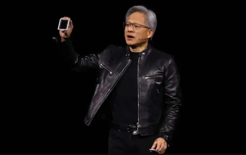
hot_img NVIDIA's Feynman platform is expected to go into mass production in 2028, with TSMC's A16 and SoIC expanding production simultaneously

According to DIGITIMES, NVIDIA's next-generation AI platform Feynman aims for mass production in the second half of 2028, utilizing TSMC's A16 process and incorporating SoIC 3D stacking and CPO technology. The Rubin generation focuses on integrating multiple small chips with HBM, while Feynman further develops towards 3D small chips, SoIC, and CPO. The report indicates that TSMC is accelerating the construction of related production capacity, with the original plan for SoIC monthly capacity to reach 20,000 pieces by the end of 2026, now updated to a target of 50,000 pieces by the end of 2027.The construction progress of TSMC's Chiayi AP7 and Tainan AP8 is also accelerating, with AP7 planned in 8 phases. P1 and P2 have entered installation, P3 and P4 have obtained construction permits, and P5 to P8 are still in planning. In addition to mass-producing Apple-specific WMCM, the factory will configure SoIC, CoPoS, and CPO production lines according to customer demand. NVIDIA has rapidly shifted its R&D and supply chain resources to the Feynman platform, and the spillover effect of TSMC's advanced packaging orders continues to expand, with Siliconware becoming the main testing and packaging factory for NVIDIA's CoWoS and CPO orders. The NVLink interconnect bandwidth of NVIDIA's Feynman platform is expected to exceed 1 PB/s, further improving from Rubin Ultra's 520 TB/s. TSMC's COUPE technology integrates EIC and PIC in 3D through SoIC to form a light engine, advancing optoelectronic conversion from traditional circuit boards to the internal packaging structure. Since 2026, NVIDIA has invested over $40 billion in building the AI ecosystem, covering areas such as models, wafer manufacturing, data centers, and optical communications.
app_icon
ChainCatcher Building the Web3 world with innovations.